


10nm, 7nm, 5nm…. Should the Chip Nanometer Metric Be Replaced?

The biggest cool factor in server chips is the nanometer. AMD beating Intel to a CPU built on a 7nm process node* – with 5nm and 3nm on the way – has been instrumental to AMD’s data center market resurgence. Nanometer cachet is incalculable: on it, companies, careers and fortunes are made and lost.
But that cachet is coming into question. As with the LINPACK benchmark for ranking HPC system performance, a growing chorus of voices is calling for other ways to assess and characterize chips.
Before further discussion, let’s define our terms. A nanometer is one billionth of a meter, also expressed as 0.000000001 or 10-9 meters (for perspective, hair grows at roughly 1 nm per second**). In chip design, “nm” refers to the length of a transistor gate – the smaller the gate the more processing power that can be packed into a given space.
Some chip technologists argue that the nanometer is too narrow a measure of chip advancement. Writing in IEEE last month, nine computer scientists from MIT, Stanford, University of California/Berkeley and Taiwan-based chip manufacturer TSMC have put forward a new “density metric” designed to be a more holistic gauge. The nanometer metric “is all but obsolete today,” they said, for not simultaneously accounting for logic, memory and packaging/integration technologies. What’s needed is to capture a broader set of system-level performance indicators, connecting “the device technology advances to system-level benefits in a comprehensive fashion while acknowledging the synergy between various components.”
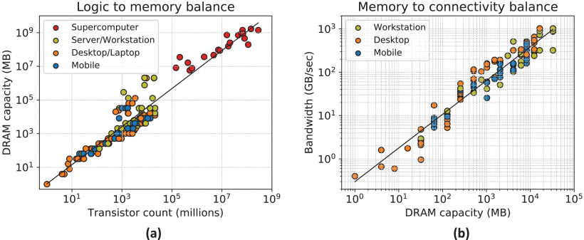
Available at https://purl.stanford.edu/jj585np1768, the data “suggest that a balanced growth between logic, memory and connectivity has been an implicit guide for computing system optimization,” according to the authors.
Classifying chips by transistor gate length – the “node number” – has been around since the 1960s. But over the past decade, “driven by competitive marketing,” the nanometer metric has been pushed, pulled and distorted in several ways, the authors stated. For one, the node number “has become decoupled from, and can be several times smaller than, the actual minimum gate length.” For another, different semiconductor manufacturers brand similar logic technologies with “different node labels, thus creating further confusion.”
They also point out that while 5nm chips are slated to go into production next year, the next-generation node will be 3nm, so “we will soon run out of nanometers for naming future generations of technologies.” More importantly, 3nm is roughly the size of about 12 atoms, so small it could create doubts that semiconductor technology advancement is nearing physical limits.
“Yet, it is a foregone conclusion that the semiconductor industry will continue to make progress,” the authors asserted, “because there are still many ways to advance semiconductor technology beyond 2-D miniaturization and also because societal demand for more capable electronic systems is insatiable.”
In place of the nm node number, the authors’ proposed “LMC density metric” would be a three-part number reflecting the relationship between density and “benefits for more advanced computing systems — the primary driver for progress in semiconductor technology.”
The three numbers:
- DL: density of logic transistors in #/mm2
- DM: bit density of main memory (currently the off-chip DRAM density in #/mm2)
- DC: density of connections between the main memory and logic (in #/mm2)
The authors said that, based on design specifics, today’s leading edge technologies can be characterized by [38M, 383M, 12K].
“These three components of the system metric contribute to the overall speed and energy efficiency of computing systems,” the authors said. “This balance is implicit in computer architectures and allows the improvement of overall system performance in an optimal fashion.” They also noted that historical data show a “correlated growth” in logic, memory and connectivity, suggesting “a balanced increase of DL , DM , and DC for the decades to come.”
The metric places particular focus on the integrations of logic, memory and connectivity, the authors said. “In addition to being consistent with historical trends and our intuition about computing systems, the LMC density metric is applicable and extensible to future logic, memory, and packaging/integration technologies.”
Acknowledging that chip vendors may “continue to use their preferred labels to market their technologies,” the authors said the LMC density metric could foster “clear communications” by serving “as a common language to gauge technology advances among semiconductor manufacturers.”
Above all, the authors said, the LMC density metric “takes the semiconductor industry out of the quandary of using the vanishing nanometer as a label to describe advancements in semiconductor technology that will remain very important to society for a very long time to come.”
* Roughly corresponding to Intel's (delayed) 10nm process node
** See comments from Phil Moriarty, professor of physics, School of Physics and Astronomy, University of Nottingham


