


Nvidia Showcases Domain-specific LLM for Chip Design at ICCAD
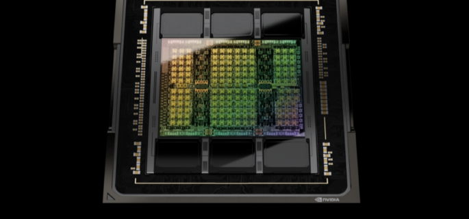
Nvidia H100 die.
This week Nvidia released a paper demonstrating how generative AI can be used in semiconductor design. Nvidia chief scientist Bill Dally announced the new paper during his keynote at the International Conference on Computer-Aided Design (ICCAD) now taking place in San Francisco.
“This effort marks an important first step in applying LLMs to the complex work of designing semiconductors,” said Dally at the event in San Francisco. “It shows how even highly specialized fields can use their internal data to train useful generative AI models.”
Mark Ren, an Nvidia research director and lead author on the paper, said “I believe over time large language models will help all the processes, across the board. Nvidia issued a blog on the work along with the paper (ChipNeMo: Domain-Adapted LLMs for Chip Design).
Designing today’s giant chips, such as Nvidia’s H100 GPU, is typically a two-year effort involving multiple engineering teams. The sudden emergence of LLM and Generative AI has triggered a wave of efforts to develop customized, domain-specific LLMs. Bloomberg’s financial LLM (BloombergGPT) is a good example.
The expectation is that domain-specific LLMS will join the EDA tool world and significantly speed and improve complex chip design. At this point ChipNeMo is an internal project for internal use only. The paper’s abstract summarizes the work nicely:
Abstract: "ChipNeMo aims to explore the applications of large language models (LLMs) for industrial chip design. Instead of directly deploying off-the-shelf commercial or open-source LLMs, we instead adopt the following domain adaptation techniques: custom tokenizers, domain-adaptive continued pretraining, supervised fine-tuning (SFT) with domain-specific instructions, and domain-adapted retrieval models.
"We evaluate these methods on three selected LLM applications for chip design: an engineering assistant chatbot, EDA script generation, and bug summarization and analysis. Our results show that these domain adaptation techniques enable significant LLM performance improvements over general-purpose base models across the three evaluated applications, enabling up to 5x model size reduction with similar or better performance on a range of design tasks. Our findings also indicate that there’s still room for improvement between our current results and ideal outcomes. We believe that further investigation of domain-adapted LLM approaches will help close this gap in the future."
 The paper authors write, “We believe that LLMs have the potential to help chip design productivity by using generative AI to automate many language- related chip design tasks such as code generation, responses to engineering questions via a natural language interface, analysis and report generation, and bug triage.”
No doubt Nvidia has self-interest here, both in strengthening its position in LLM development/provider community as well as stirring demand for its broad product portfolio. ChipNeMo was built using Nvidia’s NeMo cloud framework for LLM development and training.
Before starting the ChipNeMo project, Nvidia conducted a survey of potential LLM applications within own design teams. According to the paper, the responses fell roughly into four buckets: code generation, question & answer, analysis and reporting, and triage.
“Code generation refers to LLM generating design code, testbenches, assertions, internal tools scripts, etc.; Q & A refers to an LLM answering questions about designs, tools, infrastructures, etc.; Analysis and reporting refers to an LLM analyzing data and providing reports; triage refers to an LLM helping debug design or tool problems given logs and reports. We selected one key application from each category to study in this work, except for the triage category which we leave for further research,” according to the paper.
The paper walks through the strategy and steps taken in developing ChipNeMo, providing a rough template for others. Obviously, there are more tasks that could be tackled. In the blog Nvidia reported it has other semiconductor design projects using AI to design smaller, faster circuits and to optimize placement of large blocks.
One important lesson learned from ChipNeMo project, reported Nvidia, is that these domain-specific LLMs can be substantially small and run effectively on smaller compute platforms.
This from the bog: “On chip-design tasks, custom ChipNeMo models with as few as 13 billion parameters match or exceed performance of even much larger general-purpose LLMs like LLaMA2 with 70 billion parameters. In some use cases, ChipNeMo models were dramatically better. Along the way, users need to exercise care in what data they collect and how they clean it for use in training, Ren added.”
Link to blog, https://blogs.nvidia.com/blog/2023/10/30/llm-semiconductors-chip-nemo/
Link to paper, https://d1qx31qr3h6wln.cloudfront.net/publications/ChipNeMo%20%2824%29.pdf


