


Google TPU v5e AI Chip Debuts after Controversial Origins

The dominance of Nvidia GPUs has companies scrambling to find non-GPU alternatives, and another mainstream option has emerged with Google’s TPU v5e AI chip.
The TPU v5e is also Google’s first AI chip being mainstreamed with a suite of software and tools for large-scale orchestration of AI workloads in virtual environments. The AI chip is now available in preview to Google Cloud customers.
The new AI chip succeeds the previous-generation TPUv4, which was used to train the newer PaLM and PaLM 2 large language models used in Google search, mapping, and online productivity applications.
Google has often compared its TPUs to Nvidia’s GPUs but was cautious with the TPU v5e announcement. Google stressed it was focused on offering a variety of AI chips to its customers, with Nvidia’s H100 GPUs in the A3 supercomputer and TPU v5e for inferencing and training.
The Cloud TPU v5e is also the first Google AI chip available outside the US. The TPUv4 was available only in North America. The TPU v5e computers will be installed in the Netherlands for the EMEA (Europe, Middle East, and Africa) markets and in Singapore for the Asia-Pacific markets.
The origins of TPU v5 were mired in controversy. Researchers at Google informally announced TPU-v5 in June 2021 and, in a paper, said AI was used to design the chip. Google claimed that AI agents helped floor-plan the chip in under six hours faster than human experts. There were internal debates on the claims made in the paper, and Google fired one researcher ahead of the paper’s appearance in Nature magazine.
Academic researchers also called out Google’s claims and criticized the company for not opening it up for public scrutiny. A researcher, Andrew B. Kahng, from the University of California, San Diego, later reverse-engineered Google’s chip-design techniques and found that human chip designers and automated tools were sometimes faster than Google’s AI-only technique.
Google has maintained a silence on that controversy but has moved ahead and is building an AI empire around TPUs. The company’s large-language models are optimized to run on TPUs, and the new chips are critical to Google’s data centers as the company infuses AI features across product lines.
The performance numbers point to the TPU v5e being adapted for inferencing instead of training. The chip offers a peak performance of 393 teraflops of INT8 performance per chip, which is better than 275 petaflops on TPU v4.
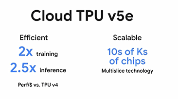
The new Google TPU v5e is more efficient and more scalable than v4, Google says.
But the TPU v5e scores poorly on BF16 performance, with its 197 teraflops falling short of the 275 teraflops on the TPU v4.
But TPU v5e could outperform the TPU v4 when conjoined in clusters. The TPU v4 could be configured in clusters of 4,096 chips, but TPU v5e can expand to hundreds or thousands more configurations and tackle even larger training and inferencing models.
Google Cloud executives Amin Vahdat and Mark Lohmeyer, in a blog entry said “the size of the largest jobs at a maximum slice size of 3,072 chips for TPU v4,” and not 4,096 chips, as previously claimed. But with TPU v5e, the company has introduced a technology called “Multislice,” which can network hundreds of thousands more AI chips together in a cluster.
Multislice “allows users to easily scale AI models beyond the boundaries of physical TPU pods — up to tens of thousands of Cloud TPU v5e or TPU v4 chips,” Google executives said.
Google has also finetuned virtual machines for TPU v5e so chips can process multiple virtual machines simultaneously. Google announced the availability of the Kubernetes service for Cloud TPU v5e and v4, which will help orchestrate AI workloads across the TPUs.
Google said the largest configuration could deploy 64 virtual machines across 256 TPU v5e clusters. The TPUs work with machine-learning frameworks that include Pytorch, JAX, and TensorFlow.
“TPU v5e is also incredibly versatile, supporting eight different virtual machine configurations, ranging from one chip to more than 250 chips within a single slice. This feature allows customers to choose the right configurations to serve a wide range of LLM and gen AI model sizes,” Google execs wrote.
Each TPU v5e chip has four matrix multiplication units, a vector, and a scalar processing unit, which are all connected to HBM2 memory.
Google’s data centers have a swap-in, swap-out high-bandwidth infrastructure with optical switches that link up AI chips and clusters. The optical interconnect allows each rack to operate independently and interconnected on the fly, and technology allows Google to quickly reconfigure the network topology depending on the application.
Google provided interesting performance comparisons to TPU v4 based on cost. The benchmark is a practical assumption of the cost of training and the size of a model. Microsoft and Google are investing billions in their data center infrastructure so companies can train and deploy larger AI models
 For every dollar, the TPU v5e is up to two times faster in training and 2.5 times inferencing times. The TPU v5e is priced at $1.2 per chip hour, while the TPU v4 is about $3.2 per hour.
“At less than half the cost of TPU v4, TPU v5e makes it possible for more organizations to train and deploy larger, more complex AI models,” the Google executives said in the blog.
Google has shared the TPU v5e configurations on its website, which are broken up into training and inference pages.
The training model is for “transformer, text-to-image, and Convolutional Neural Network (CNN) training, finetuning, and serving,” Google said on its website.
Google separately announced that the A3 supercomputer, which has up to 26,000 Nvidia H100 GPUs, will be generally available next month. The A3 is designed for companies working with massive large-language models, including financial, pharmaceutical, and engineering firms.
Google’s TPU compute infrastructure was mentioned as an ace up its sleeve by research firm SemiAnalysis in a post on August 27. The post largely addressed “GPU Poors,” or companies that do not have ready access to GPUs that are in heavy demand. The post elicited an unprovoked response from Sam Altman, the CEO of OpenAI, who wrote, “Incredible google got that SemiAnalysis guy to publish their internal marketing/recruiting chart lol.” The exchange was largely friendly banter with no serious punches thrown.
OpenAI’s infrastructure is swimming in GPUs in part thanks to Microsoft’s AI infrastructure, which has doubled down on graphics chips from Nvidia. Cloud providers charge a significant premium to access Nvidia’s A100 and H100 GPUs. But unlike Microsoft, Google is not putting its eggs in one basket, and adding TPUs allows a range of AI offerings at multiple price points.
Amazon AWS has also integrated its homegrown Trainium and Inferentia chips for training and inferencing. Intel has a $1 billion pipeline of orders for its AI chips, which include Gaudi2 and Gaudi3 chips.
This article first appeared on sister site HPCwire.


