


Industry Heavyweights Launch UCIe Consortium to Drive Chiplet Interconnect Standard
A new industry consortium aims to establish a die-to-die interconnect standard – Universal Chiplet Interconnect Express (UCIe) – in support of an open chiplet ecosystem. Intel Corporation donated the UCIe 1.0 spec, which was then ratified by the 10 promoter members that span chip companies, semiconductor suppliers and cloud service providers.
The charter roster consists of AMD, Arm, Advanced Semiconductor Engineering, Inc. (ASE), Google Cloud, Intel, Meta (Facebook’s parent company), Microsoft, Qualcomm, Samsung and TSMC. Nvidia is notably absent from the grouping, despite exploring a chiplet path for its next-generation GPU designs.
The UCIe 1.0 specification is a complete standardized die-to-die interconnect, encompassing a physical layer, protocol stack, software model, and compliance testing, the consortium said. It natively maps PCI Express (PCIe) and Compute Express Link (CXL) protocols. The spec will enable end users to mix and match dies and other chiplet components from multiple sources with different packaging options.
As with other chiplet implementations, there can be compute cores fabbed on the most advanced process node, while the memory and IO controller, for example, can be a prior generation process. This not only optimizes for semiconductor costs, it saves the expense of porting that IP over and validating it again.
An optimized physical layer is defined for both standard (2D) packaging, and advanced (2.5D) packaging as shown in the figure below. Depicted on the right are different packaging options in use by some of the founding companies, namely Intel and TSMC.
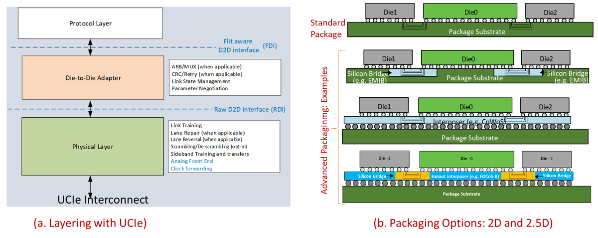
Source: UCIe Consortium
CXL and PCIe address a number of use cases. “With PCIe and CXL, SoC construction, link management, and security solutions that are already deployed can be leveraged to UCIe,” notes a consortium white paper, written by UCIe Chair (and Senior Intel Fellow) Debendra Das Sharma. “The usage models addressed are also comprehensive: data transfer using direct memory access, software discovery, error handling, etc., are addressed with PCIe/CXL.io; the memory use cases are handled through CXL.Mem; and caching requirements for applications such as accelerators are addressed with CXL.cache. UCIe also defines a ‘streaming protocol’ which can be used to map any other protocol.”
In an interview with HPCwire, Das Sharma discussed the motivations for the on-package integration of chiplets. “What we're seeing is that a lot of our designs are hitting the reticle limit as the demand for processing is insatiable, so it's easier for us – and by 'us' I mean the broader industry – to build smaller chiplets and stitch them together on the package so that they act as a single entity. So this is a scale up kind of solution.”
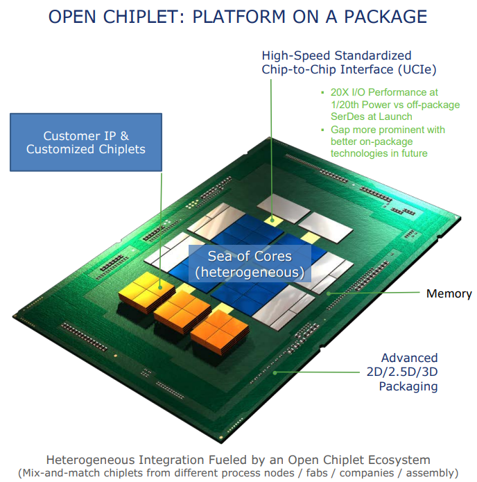
Source: UCIe Consortium
Enabling the construction of SoCs that exceed maximum reticle size is a key aim of the standard, which also aims to reduce time-to-solution by enabling die reuse, lower portfolio costs, and facilitate bespoke solutions. “You can basically do a mix and match of different dies depending on what the customer needs are, so that you can deliver a purpose-built solution out of a standard set of dies,” said Das Sharma.
One of the most interesting things about this announcement: the coterie of competitors who are coming together to drive the standard. This continues the trend of sophisticated coopetition plays that we saw, for example, with Intel's March 2021 announcement of expanded partnerships with competitors TSMC and IBM. The more challenging (read: expensive) that design and packaging becomes, the greater the need for collaboration.
Will UCIe lay the way for devices from competing companies to be combined on an SoC? That's already happening with Intel's forthcoming Ponte Vecchio GPU, which is using TSMC's N5 compute dies in addition to a number of other dies fabbed by Intel. The new standard creates the conditions for more “strange bedfellows,” and, in fact, the motivation is baked in.
“The entire purpose of UCIe is to create an open and interoperable chiplet ecosystem," said Das Sharma. “We have a well-defined specification that encompasses electrical (including bump map), die-to-die adapter, protocol mapping, sideband, and configuration register that allows for seamless interoperability between UCIe components. This is similar to existing successful standards like PCIe and CXL. So yes, you can have a package where components from various companies can interoperate with each other.”

Source: UCIe Consortium
The UCIe spec supports two broad usage models: package level integration and off-package connectivity. In the former, components that are attached at the board level – such as memory, accelerators, or networking devices – can be integrated at the package level. The second implements off-package connectivity using different types of media (optical, electrical cable, mmWave) and UCIe retimers. The retimers transmit the underlying protocol (PCIe, CXL) out to the rack or pod level, and enable resource pooling or sharing, thus facilitating resource disaggregation.
The consortium claims a 20-fold boost in IO performance at 1/20th the power envelope versus off-package SerDes at launch. The chart below shows key performance indicators.
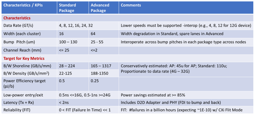
Source: UCIe Consortium
The new consortium follows other standards that have been jump-started by Intel, such as CXL, the PCI bus, PCI Express and USB, which have evolved into fully open and independent efforts.
The point is underscored by Jim Pappas, the Intel director and CXL chair acting as a consultant to the UCIe consortium. “Yes, Intel put the pen to the spec, but this is a consortium-owned spec at this point, and all future work on this is not [under the direction of] any one company,” he said. “There are 10 promoters, and the promoters are the ones who make the decisions on what goes into the spec. We each get one vote. Any company can join (within the scope of U.S. laws).”
“The nice thing about starting with a spec is that much of the early decisions have been made,” Pappas added. “You know what it is and where it's going. The end result won’t necessarily be what was originally donated; it will evolve over time, it'll get faster, it will have new capabilities, new protocols – the industry will evolve.”
Das Sharma likewise envisions a long life ahead. “My expectation is we have got decades of innovations that we are going to do with this," he said. “This is really how SoCs are going to be built, from my perspective.”
The founding companies are in the process of finalizing incorporation as an open standards body, and expect to do so by year end. The member companies will then begin work on the next generation of UCIe technology, covering the design of the chiplet form factor, as well as management and enhanced security.
UCIe "Promoters" at launch
Intel, AMD and the other founding companies commented on the launch of the consortium.
“Integrating multiple chiplets in a package to deliver product innovation across market segments is the future of the semiconductor industry and a pillar of Intel’s IDM 2.0 strategy,” said Sandra Rivera, executive vice president and general manager, data center & AI, at Intel. “Critical to this future is an open chiplet ecosystem with key industry partners working together under the UCIe Consortium toward a common goal of transforming the way the industry delivers new products and continues to deliver on the promise of Moore’s Law.”
“AMD is proud to continue our long history of supporting industry standards that can enable innovative solutions addressing the evolving needs of our customers,” said Mark Papermaster, executive vice president and chief technology officer, AMD. “We have been a leader in chiplet technology and welcome a multi-vendor chiplet ecosystem to enable customizable third-party integration. The UCIe standard will be a key factor to drive systems innovation leveraging heterogeneous compute engines and accelerators that will enable the best solutions optimized for performance, cost, and power efficiency.”
For more, see the launch announcement on the consortium website.


