


Marvell Demonstrates Industry’s First 3nm Data Infrastructure Silicon
SANTA CLARA, Calif., April 19, 2023 -- Marvell Technology, Inc., a leader in data infrastructure semiconductor solutions, has demonstrated high-speed, ultra-high bandwidth silicon interconnects produced on Taiwan Semiconductor Manufacturing Company's (TSMC) 3-nanometer (3nm) process. Marvell's industry-first silicon building blocks in this node include 112G XSR SerDes (serializer/de-serializer), Long Reach SerDes, PCIe Gen 6 / CXL 3.0 SerDes, and a 240 Tbps parallel die-to-die interconnect.
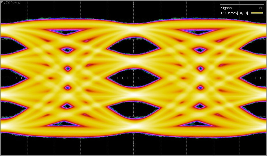
The blue eye diagram, PCIe Gen 6 SerDes (@ 64Gb/s), represents high-performance signals transmitted by Marvell’s 3nm SerDes optimized for PCIe Gen 6 / CXL 3.0. This is an industry-first. The vertical height, size, and relative symmetry of the eyes indicate the mitigation of noise and bit errors.
The new building blocks are part of Marvell's continued execution of its strategy to develop a comprehensive silicon IP portfolio for designing chips that will radically increase the bandwidth, performance, and energy efficiency of next-generation data infrastructure. These technologies also support all semiconductor packaging options from standard and low-cost RDL (Redistribution Layers) to silicon-based high-density interconnect.
Marvell was also the first data infrastructure silicon supplier to respectively sample and commercially release the industry-leading 112G SerDes and has been a leader in data infrastructure products based on TSMC's 5nm process.
SerDes and parallel interconnects serve as high-speed pathways for exchanging data between chips or silicon components inside chiplets. Together with 2.5D and 3D packaging, these technologies will eliminate system-level bottlenecks to advance the most complex semiconductor designs. SerDes also help reduce pins, traces and circuit board space to reduce cost. A rack in a hyperscale data center might contain tens of thousands of SerDes links.
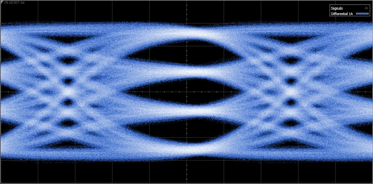
The orange eye diagram, 112G XSR SerDes (@ 113Gb/s), represents the signals from Marvell’s 3nm low latency SerDes optimized for 112G XSR. This is an industry-first. The vertical height, size, and relative symmetry of the eyes indicate the mitigation of noise and bit errors.
The new parallel die-to-die interconnect, for example, enables aggregate data transfers up to 240 Tbps, 45% faster than available alternatives for multichip packaging applications. To put it in perspective, the interconnect transfer rate is equivalent to downloading 10,000 HD movies every second, although over a distance of only a few millimeters or less.
Marvell incorporates its SerDes and interconnect technologies into its flagship silicon solutions including Teralynx switches, PAM4 and coherent DSPs, Alaska Ethernet physical layer (PHY) devices, OCTEON processors, Bravera storage controllers, Brightlane automotive Ethernet chipsets, and custom ASICs. Moving to a 3nm process enables engineers to lower the cost and power consumption of chips and computing systems while maintaining signal integrity and performance.
"Interconnects are taking on heightened importance as clouds and other computing systems grow in size, complexity and capability. Our advanced SerDes and parallel interfaces will play a significant role in providing a platform for developing chips with best-in-class bandwidth, latency, bit error rate, and power efficiency for meeting the demands of AI and other complex workloads," said Raghib Hussain, president of products and technologies at Marvell. "We are proud to be able to deliver such advances on TSMC's 3nm technology and take semiconductor designs to the next level for our customers around the world."
"Bandwidth is the lifeblood of the cloud. Service providers are growing their network capacity by approximately 50% per year in the cloud and by over 100% for AI applications," said Alan Weckel, co-founder of 650 Group. "Marvell's successful production of 3nm SerDes and interconnects marks the latest step in helping cloud service providers to stay ahead of the ever-escalating demand for higher speeds and more traffic."
"We congratulate Marvell on the achievement of this important silicon development milestone in the industry's cutting-edge 3nm process technology," said Joachim Peerlings, general manager of Keysight's Communications Solutions Group. "We are very pleased with our progress on the broader industry enablement and excited to work with top technology innovators like Marvell to showcase next generation interconnect technologies that will help push the boundaries of data infrastructure silicon design, performance and energy efficiency."
About Marvell
To deliver the data infrastructure technology that connects the world, Marvell (NASDAQ: MRVL) is building solutions on the most powerful foundation: our partnerships with our customers. Trusted by the world's leading technology companies for over 25 years, we move, store, process and secure the world's data with semiconductor solutions designed for our customers' current needs and future ambitions. Through a process of deep collaboration and transparency, we're ultimately changing the way tomorrow's enterprise, cloud, automotive, and carrier architectures transform—for the better. Marvell and the M logo are trademarks of Marvell or its affiliates. Please visit www.marvell.com for a complete list of Marvell trademarks. Other names and brands may be claimed as the property of others.
Source: Marvell


