


Ayar Labs Demonstrates Optical Interconnect on GLOBALFOUNDRIES’ Photonics Manufacturing Process
SANTA CLARA, Calif., Dec. 2, 2020 -- As part of a multi-year technology and manufacturing partnership, Ayar Labs has successfully demonstrated its patented monolithic electronic/photonic solution on GLOBALFOUNDRIES (GF) next generation photonics solution based on its 45nm platform. This is an industry first and key milestone in providing chip-to-chip optical connectivity at scale for data-hungry applications such as artificial intelligence, high performance computing, cloud, telecommunications and aerospace.
The two companies began working together in 2015 with a commitment to collaborate and commercialize differentiated silicon photonics solutions for greenfield applications that would require extreme bandwidth density (high data throughput in a small physical package) at low latency and high energy efficiency.
“Ayar Labs has been perfecting our micro-ring based monolithic electronic/photonic solution for nearly a decade. But the true commercial potential is realized when coupled with a 300mm semiconductor fabrication process that delivers the performance, reliability, and cost advantages that we and our customers require,” says Charles Wuischpard, CEO, Ayar Labs. “This is yet another industry-first result that solidifies our leadership for this market opportunity.”
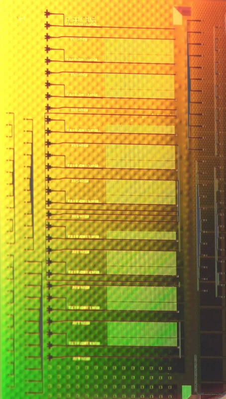
Ayar's TeraPHY high-density electronic-photonic chiplet
“Ayar Labs is an important partner of GLOBALFOUNDRIES,” says Anthony Yu, Vice President of Silicon Photonics at GF. “As collaborators, we’ve incorporated their requirements for PDK and process optimizations while providing early access to our next generation process. Together, we will unlock a larger market opportunity and realize chip-to-chip optical I/O solutions that will enable higher bandwidth and faster connection for high performance compute applications.”
Over the last 18 months, Ayar Labs has been working with select semiconductor manufacturers, systems builders, and end users on co-design partnerships. The company is now announcing an expanded sampling program of its next generation chiplet developed on GF’s latest silicon photonics manufacturing process.
Dr. Mark Wade, President and CTO of Ayar Labs, will be sharing details of this industry first demonstration at ECOC 2020 as part of his presentation on ‘Silicon photonic chiplets for chip-to-chip communications’ on Tuesday, December 8, from 16:20 – 16:40 (CET). A video of the demonstration will also be made available at this time.
About Ayar Labs
Ayar Labs is disrupting the traditional performance, cost, and efficiency curves of the semiconductor and computing industries by driving a 1000x improvement in interconnect bandwidth density at 10x lower power. Ayar Labs’ patented approach uses industry standard cost-effective silicon processing techniques to develop high speed, high density, low power optical based interconnect “chiplets” and lasers to replace traditional electrical based I/O. The company was founded in 2015 and is funded by a number of domestic and international venture capital firms as well as strategic investors. Ayar Labs was also recently named one of the 10 Hottest Semiconductor Startups of 2020 by CRN. For more information, visit www.ayarlabs.com.
About GLOBALFOUNDRIES
GLOBALFOUNDRIES (GF) is a leading specialty foundry. GF delivers differentiated feature-rich solutions that enable its customers to develop innovative products for high-growth market segments. GF provides a broad range of platforms and features with a unique mix of design, development and fabrication services. With an at-scale manufacturing footprint spanning the U.S., Europe and Asia, GF has the flexibility and agility to meet the dynamic needs of customers across the globe. GF is owned by Mubadala Investment Company. For more information, visit www.globalfoundries.com.
Source: Ayar Labs


