


Google, SkyWater Partner on Open ASIC Designs
via Shutterstock
Google along with chip foundry partner SkyWater Technology and an IC design kit vendor are joining forces to offer what they promote as “open source manufacturing of custom ASICs.”
The Google-sponsored Multi-Project Wafer (MPW) initiative, one of several being launched by chip makers, is billed as an open source foundry process design kit. The partners along with chip design specialist Efabless Corp. said Thursday (Nov. 12) they are now accepting IC design submissions from which selected chips will be processed during the initial wafer production run. Unlike Field Programmable Gate Array (FPGA) integrated circuits, which can be reprogrammed, ASICs (Application Specific Integrated Circuit) are designed and manufactured to serve one purpose and cannot be reprogrammed for changing uses.
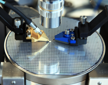
SkyWater, the pure play semiconductor foundry based in Bloomington, MN, said ASIC designs based on the open source process design kit would be selected and manufactured using its 130-nm mixed-signal CMOS technologies.
A portal launched by San Jose-based Efabless includes a workflow that allows users to submit candidate designs for the MPW effort. SkyWater has counted more than 1,700 downloads, and the portal will accept IC design submissions through Nov. 30.
The process design kit is available here.
The portal allows chip designers to “collaborate to create and verify ASICs and supporting IP,” said Mohamed Kassem, chief technology officer and co-founder of Efabless. “The open source model multiplies the collaboration in semiconductor chip design. Over time we expect to see advanced—and high quality—designs coming from the open source community.”
The chip design initiative seeks to develop an open source manufacturing supply chain for custom ASICs. That effort is being promoted by the Free and Open Source Silicon Foundation, among others.
For its part, Google (NASDAQ: GOOGL) said cloud-based platforms would make it easier and cheaper to design custom silicon that is otherwise relatively pricey compared to high-volume devices. For example, Google is a founding member of the RISC-V Foundation.
Efabless released an open source design stack available under an Apache 2.0 license. The OpenLane framework is an automated register transfer level design tool that supports SkyWater’s 130-nm process design kit.
The open source “shuttle” initiative aims to allow chip designers to “push the state-of-the-art without having to reconcile the risk associated with the cost of fabrication,” EFabless said. That’s because Google will cover fabrication, packaging, evaluation and shipping costs.
According to John Kent, SkyWater executive vice president of technology development and design enablement, the open source design kit is expected to generate “re-usable [intellectual property] which will amplify idea generation and feed product development that is ongoing in the IoT and industrial space.”
The partners said they will accept another round of design submissions in 2021.
SkyWater’s is among a growing list of multi-project wafer programs sponsored by various chip manufacturers, including GlobalFoundries, Tower Semiconductor and others.


