


AI Chip Start-up Groq to Detail Technology Progress in Fall
AI chip startup Groq announced this week it had closed its most recent funding round, saying the new investments will help it double in size by the end of this year and double again by the end of next year as it transitions to commercial development. Groq’s new neural network chip – the Tensor Streaming Processor – is well along in development and designed to speed inferencing and consume low power. Among the new investors are D1 Capital, announced yesterday, and TDK Ventures, announced last week.
The amount of the new investments was not disclosed (see Groq release) but it’s no doubt good news for the start-up. Groq is one of many newcomers seeking to make waves in the AI market. It was started in the 2017 timeframe by former Google employees including Groq CEO Jonathan Ross who participated in TPU development at Google. Bill Leszinske, VP of products and marketing, told HPCwire more details about the technology roadmap and early customers would be discussed at the AI Hardware Summit this fall.
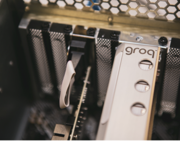
 “Jonathan Ross will specifically talk about the products that we’re shipping and have shipped to customers,” Leszinske said. “We have our core piece of silicon and the initial software stack that we’ve been working on. That has shipped as a PCIe add-in card that goes into servers and very high-end workstations.” Groq is currently targeting a few market segments, in particular those with low power and high performance requirements such as autonomous vehicles. He cited HPC more broadly as a target market as well as power-hungry hyperscaler datacenters. Leszinske said several government labs would be working with the new chip. That wouldn’t be surprising given many national labs – Argonne, for example – have set up AI chip test beds to assess new devices.
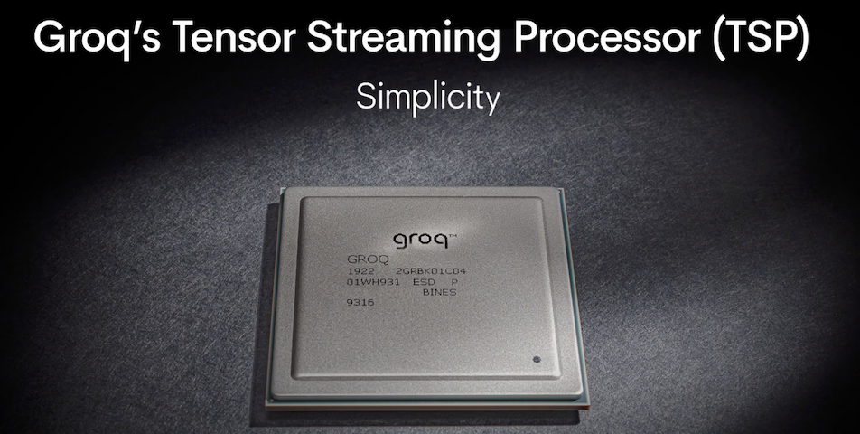
The TSP is being fabbed on a 14nm process by Global Foundaries and a fairly thorough description of its architecture was presented at IEEE’s 2020 International Symposium on Computer Architecture (link to paper).
Briefly, the idea is to remove some of the overhead (instructions) required to use general purpose microprocessors by physically moving and reorganizing functional elements (e.g. with needed memory and support located nearby). “Instead of creating a small programmable core and replicating it dozens or hundreds of times, the TSP houses a single enormous processor that has hundreds of functional units. This novel architecture greatly reduces instruction-decoding overhead, and handles integer and floating-point data, which makes delivering the best accuracy for inference and training a breeze,” says Groq.
Proximity, reduced number of instructions per op required, and efficient data flow all work together to reduce latency and increase performance, says Groq. Here’s a brief portion of the description of the architecture excerpted from the Groq paper:
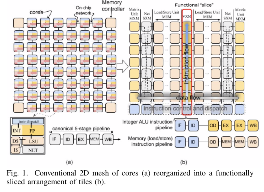
“To understand the novelty of our approach, consider the chip organization shown in Figure 1(a). In a conventional chip multiprocessor (CMP) each “tile” is an independent core which is interconnected using the on-chip network to exchange data between cores. Instruction execution is carried out over several stages: 1) instruction fetch (IF), 2) instruction decode (ID), 3) execution on ALUs (EX), 4) memory access (MEM), and 5) writeback (WB) to update the results in the GPRs. In contrast from conventional multicore, where each tile is a heterogeneous collection of functional units but globally homogeneous, the TSP inverts that and we have local functional homogeneity but chip-wide (global) heterogeneity.
“The TSP reorganizes the homogeneous two-dimensional mesh of cores in Figure 1(a) into the functionally sliced microarchitecture shown in Figure 1(b). In this approach, each tile implements a specific function and is stacked vertically into a “slice” in the Y-dimension of the 2D on-chip mesh. We disaggregate the basic elements of a core in Figure 1(a) per their respective functions: instruction control and dispatch (ICU), memory (MEM), integer (INT) arithmetic, float point (FPU) arithmetic, and network (NET) interface, as shown by the slice labels at the top of Figure 1(b).
“In this organization, each functional slice is independently controlled by a sequence of instructions specific to its on-chip role. For instance, the MEM slices support Read but not Add or Mul, which are only in arithmetic functional slices (the VXM and MXM slices).”

The company reports the following specs:
- INT8 – 1PetaOp/s @ 1.25GHz
- FP16 – 250mTFLOPS @ 1.25GHz
- Transistors – 26.8B transistors
- Process – 14nm
- SRAM – 220MB on-die
- Memory Bandwidth – 80TB/s on-die
- Host Interface – PCIe Gen 4 x 16 31.GB/s in each direction
- C2C Interface – Up to 16 chip-to-chip interconnects
- Driver – Open source, simple stack
- ECC – End to end chip protection
One question is around programming required to take advantage of the architecture. The company is still developing tools.
Leszinske said, “We have two efforts. One is this low API that gives folks high control over implementing exactly what they want and getting the most performance out of the hardware. In addition to that, we are working on a compiler. Given customer interest we had to prioritize the Groq API over the compiler as our first set of deliverables. So as we’re releasing software to customers, which again, we’ll talk about at the end of September publicly, we are using the Groq API as the initial development platform for customers. We’ll talk about the compiler later on in the year, as we start to ramp some early customers.”
Groq has also struck a deal with HPC cloud specialist Nimbix which presumably would become both a development platform and deployment platform.
Link to Groq video on its architecture: https://www.youtube.com/watch?time_continue=82&v=pb0PYhLk9r8&feature=emb_logo


