


Nvidia Launches Ampere GPU with Up to 20X the AI Performance
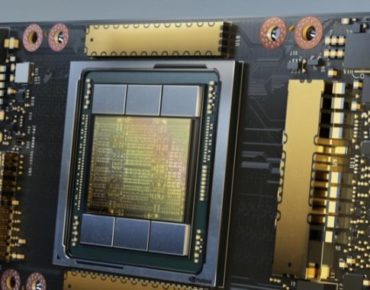
Nvidia Ampere A100 GPU
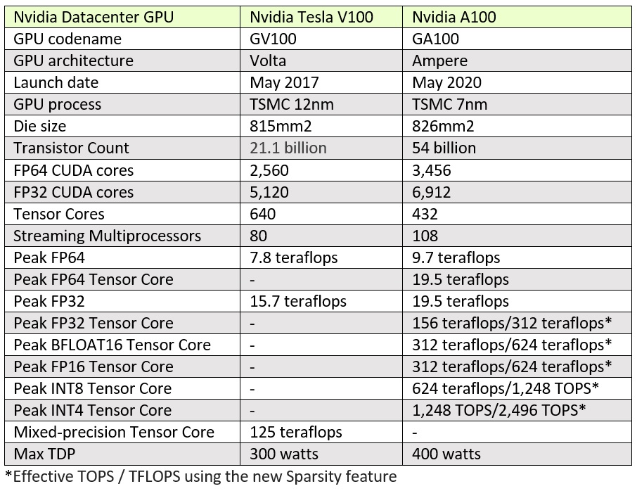
Nvidia’s first Ampere-based graphics card, the A100 GPU, packs a whopping 54 billion transistors on 826mm2 of silicon, making it the world’s largest seven-nanometer chip. Launched today during a pre-recorded “kitchen keynote” from Nvidia chief Jensen Huang, the Ampere architecture follows in predecessor Volta’s footsteps, a mega-GPU that turns up the dial on transistors, AI specialization and overall performance. Both the 12nm Volta and the 7nm Ampere are manufactured by TSMC.
Peak single precision performance gets a theoretical 10-20X boost over older brother Volta (V100) with the addition of TensorFloat-32 (TF32) tensor cores. HPC workloads benefit from a 250 percent increase in peak double-precision floating point performance owing to new IEEE-compliant tensor core instructions for HPC processing.
Other new features include:
• Multi-instance GPU (aka MIG) which enables a single A100 GPU to be partitioned into as many as seven separate GPUs.
• Third-generation Nvidia NVLink fabric, which doubles the high-speed connectivity between GPUs.
• And structural sparsity, which introduces support for sparse matrix operations in Tensor cores, and accelerates them by two times.
Here’s a comparison chart showing key specs for Volta V100 and Ampere A100 GPUs:
Ampere doubles down on Nvidia’s single universal GPU strategy introduced with the Volta architecture that supported HPC, AI and graphics. “[With Ampere A100], instead of having a whole bunch of Volta GPU servers, a bunch of T4 GPU servers, and CPU servers, all of that can now be run on one unified Ampere server,” said Huang in a briefing held for media yesterday.
“This is unquestionably the first time that we’ve unified the acceleration workload of the entire datacenter into one single platform,” Huang added. “You know, everything from video analytics to image processing to voice to training to inference, the data processing is now one unified server.”
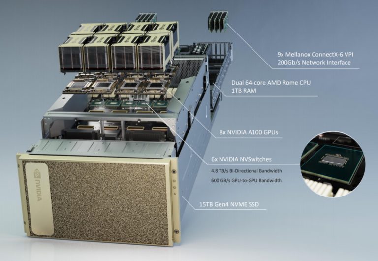
Here Huang is referring to the new DGX machine, also launched today. The DGX A100 is powered by eight A100 GPUs that together provide 320GB of memory with 12.4TB per second bandwidth. Six NVSwitches with third-generation NVLink fabric connect the GPUs, providing 4.8TB per second of bi-directional bandwidth. Each DGX 100 system offers nine Mellanox ConnectX-6 200Gb/s network interfaces and 15TB Gen4 NVMe storage.
Nvidia DGX A100 with nearly 5 petaflops FP16 peak performance (156 FP64 Tensor Core performance)
With the third generation “DGX,” Nvidia made another change not highlighted in yesterday’s briefing or other press materials, save for one slide. Instead of two Broadwell Intel Xeons, the newest DGX sports two 64-core AMD Epyc Rome CPUs. The move could signal Nvidia’s pushback on Intel’s emerging GPU play or may have been motivated by AMD’s price-performance story.
An Arm CPU option is also in the wings now, and with strong ongoing development activity around GPU-accelerated Arm, we would not be surprised to see another CPU shakeup in a fourth-gen DGX. Nvidia could choose an Arm server chip from Marvell or Ampere (hmm) or it could decide to go full-bore and add an internally-developed Arm CPU to its ever-growing stack.
Speaking of Nvidia's stack -- with the introduction of DGX-1 four years ago on through the announced (and now completed) acquisition of Mellanox, Nvidia shied away from the systems-maker appellation, aware of the potential conflict with OEM partners. That reluctance seems to have have diminished.
“We develop vertically fully integrated systems to pioneer new form factors of computers,” said Paresh Kharya, director of product management for Nvdia’s datacenter and cloud platforms in the same media briefing. “We open the entire system as well and turn them into elemental building blocks. So our ecosystem, the entire industry can buy pieces or whole,” he continued, referencing the HGX A100 design that will be supported by partnering cloud service providers and server makers.
Huang later added, “Nvidia is really a datacenter scale computing company. We used to be a PC company 30 years ago, then we became a workstation company, then we became a server company, and we ultimately worked our way into the datacenter. But the future of computing: the datacenter is the computing unit. The future of computing is really datacenter scale; applications are going to run in the entire datacenter all at the same time.”
Nvidia also announced the creation of the DGX A100 Superpod, spanning 140 DGX A100 systems (1,120 GPUs), 170 Mellanox Quantum 200G IB switches, 280 TB/s network fabric (over 15km of optical cable), and 4 petabyes of all-flash networked storage. The entire system delivers nearly 22 petaflops of peak double-precision performance (700 petaflops of “AI computing”) and was built in under three weeks, Nvidia said.
Nvidia has added four Superpods to its internal supercomputer Saturn-V, boosting its total “AI supercomputing” capacity to nearly 5 exaflops, which Nvidia says makes Saturn-V the fastest AI supercomputer in the world. The total double-precision capacity of all those GPUs comes out to about 93 peak petaflops, but Jensen clarified that Saturn-V is not really one system. It sits in four different locations under one management interface. Nvidia uses the system for software development pertaining to computer graphics, robotics, self-driving cars, healthcare and its new recommender system, Merlin.
The DGX A100 lists at $199,000 and is shipping now. The first order went to the U.S. Department of Energy’s Argonne National Lab, which is using the cluster for AI and computing to better understand and fight COVID-19. Other early adopters in the HPC research community include Indiana University, Jülich Supercomputing Center, Karlsruhe Institute of Technology, Max Planck Computing and Data Facility, and NERSC at the DOE’s Berkeley National Laboratory.But Nvidia has another reason for building Saturn-V. “If we’re a datacenter scale company developing chips, systems and software at the datacenter scale, it stands to reason that we should build it ourselves,” said Huang.
There is robust partner support. The list of cloud service providers and systems builders expected to integrate the A100s includes Alibaba Cloud, Amazon Web Services (AWS), Atos, Baidu Cloud, Cisco, Dell Technologies, Fujitsu, GIGABYTE, Google Cloud, H3C, Hewlett Packard Enterprise, Inspur, Lenovo, Microsoft Azure, Oracle, Quanta/QCT, Supermicro and Tencent Cloud.
The HGX A100 reference design, the backbone of the DGX A100, comes in a four- and an eight-GPU configuration. The four-GPU HGX A100 offers full interconnection between GPUs with NVLink, while the eight-GPU version provides full GPU-to-GPU bandwidth through NVSwitch. With the new multi-instance GPU (MIG) architecture, the Ampere servers, as we heard Huang call them, can be configured as 56 small GPUs for inferencing or as eight GPUs working together for training or HPC workloads.


