


Photonics Chiplet Startup Touts Terabit/Second I/O Bandwidth, 10X Lower Power
Silicon startup Ayar Labs continues to gain momentum with its optical chiplet technology that puts advanced electronics and optics on the same chip using standard CMOS fabrication. At Hot Chips 31 in Stanford, CA, this week, Ayar will show results of its work with DARPA (the U.S. Department of Defense's Defense Advanced Research Projects Agency) and Intel on an FPGA chiplet integration platform.
Ayar, with offices in Emeryville and Santa Clara, CA, recently taped out its 11th generation “AL11” electrical-to-optical I/O chiplet, the basis for its commercial product, called TeraPHY, which the company says will enable optical I/O bandwidth capability in excess of a Terabit/sec at 10X lower power than today’s Gigabit/sec I/O solutions.
TeraPHY will be integrated with other silicon technology partners’ designs into multi-chip module (MCM) computing products. In a stroke of good timing for Ayar – which expects early system deployments and prototypes in “reasonable volume” in 2020 – there’s something of an MCM/chiplet revolution afoot. Chipmakers, such as Intel and AMD, are turning to the modular packaging approach to sidestep Moore’s law.
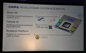
Ayar has worked closely with Intel’s Programmable Solutions Group as part of the DARPA CHIPS (Common Heterogeneous Integration and IP Reuse Strategies) project. At Hot Chips, the company will show its 10th gen chiplet installed in an Intel FPGA package with an Intel Stratix 10 die; and it will also announce its support for the Advanced Interface Bus (AIB) protocol.
ERI Summit (July 16, 2019)
Intel’s Senior Principal Engineer Sergey Shumarayev previewed the new technology at DARPA’s ERI Summit last month. The Ayar Labs chiplet connects to the Intel Stratix 10 FPGA die via the AIB interface using Intel’s EMIB packaging. The Jariet Technologies’ millimeter wave chiplet gets information in through RF, passes that information to the FPGA for pre-processing and that gets shipped out optically via the Ayar Labs chiplet.
The University of Michigan chiplet functions as an AI accelerator. Ayar Labs is not directly involved in the University of Michigan research project, but Ayar Labs Chief Scientist and Co-Founder Mark Wade noted the AI chiplet illustrates the versatility of this type of integration.
“This chiplet package ecosystem allows someone to put in an AI accelerator chip and interface to the FPGA, and then also on the other side interface to our high performance optical IO chip; there’s a kind of transformative joint solution coming together that can be enabled by this emerging ecosystem,” said Wade, who will be presenting at Hot Chips on Tuesday.
Ayar has been working with Intel to evolve AIB — the wide, parallel PHY-level interface that Intel open sourced to help spur chiplet adoption. Freely available on GitHub, AIB is being driven as an open industry standard for enabling low-latency, power-efficient direct chiplet-to-chiplet communication.
Ayar also continues to work on support for serial interfaces, like SerDes — an approach of course that has a lot of momentum behind it. Wade said Ayar’s roadmap now includes a provision for both wide parallel implementations, such as AIB, as well as serial implementations, but he says they are getting the most traction with the wide parallel approach.
Ayar Labs CEO Charlie Wuischpard, who joined the company in November 2018, after heading HPC at Intel for a number of years, told HPCwire that while the FPGA solution being demoed this week is emerging as an Intel technology, the opportunity extends beyond working with a single vendor.
“The fact that the government is standardizing on an electrical interface makes this really suitable for anybody else to pick up and run with,” he said. “We’ve been getting a ton of interest from across the industry as there’s this greater recognition that optical I/O creates whole new sets of opportunities.
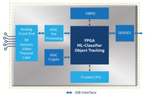
A possible heterogeneous system in package (SiP) with sensors, proprietary ASIC, FPGA, CPU, memory and I/O using AIB as the chiplet interface. (Source: Intel)
The FPGA demonstration targets phased array radar applications, which is an important market target for Ayar Labs along with 5G, but Hugo Saleh, vice president of marketing and business development, who also made the jump from Intel, told HPCwire they anticipate another killer app: high-end HPC and AI. Picture, for example, an Nvidia DGX-2 type-box, but instead of the NVLinks, there would be 16 GPUs or AI chips connected by optical interfaces, and then multiple boxes could be connected using optical instead of switched fabrics.“One of the really interesting things about our technology is not just the innovative optical chiplet that goes in the package, but once you’re relieved of the constraints that are currently in place in system designs around the power and packaging and cooling to drive the massive signals, and that’s the bandwidth over copper, then you can create brand new system architectures,” said Wuischpard.
Potential use cases extend to any server with a PCIe card in it. “We’ve got a prototype design where essentially you could take a GPU or an FPGA or an ASIC and build a system the size of a whole rack or maybe multiple racks all optically connected that far expands beyond the 16 GPUs currently supported [in the DGX2],” said Saleh.
The glueless, point-to-point interconnect approach applies for standard two-socket servers, he added. Ayar Labs foresees using optical to create supernodes where every element of the system can talk to every other element of the system, versus going up through a switch.
“We’ve reviewed this with several of the large hyperscale providers and the day we have this capability, they want to start testing it,” said Wuischpard. “We have to be able to first produce our single instance of optically connected FPGA as a first step, but we very rapidly want to move to these new system designs that use optical I/O in a new way.”
AI applications and graph analytics are clamoring for this kind of memory semantic type architecture, and government agencies are looking to leverage the technology for advanced threat intelligence, for identifying patterns in vast and disparate data sets and for tracking objects—like airplanes and drones-in real-time.
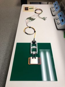
Co-packaged Stratix 10 FPGA and TeraPHY chiplets with fiber connected (courtesy: Ayar)
Ayar has in its pipeline a graph analytics design win that is using four Ayar chiplets per socket with each one of those chiplets putting out 1.3 Terabits per second of data. “That’s an aggregate of over 5 Terabits per second out of package and the only way they can do this is with optical,” Saleh stated.
Ayar Labs works closely with GlobalFoundries, a trusted foundry for the U.S. government. The TeraPHY chips are being manufactured using GloFo’s 45 nanometer RF SOI (Radio Frequency Silicon on Insulator) process, currently at its East Fishkill, NY, facility.
Each optoelectronic chip spans an area of approximately five by eight millimeters. Wade said the sizing takes into account how the chips line up with the Intel FPGA. The Intel chip is a full reticle FPGA die, about 25 millimeters on one edge, and the entire east-west side of that edge has the AIB interface on it. That allows up to three Ayar dies to abut each of those edges, to connect up to the AIB interface and escape all that bandwidth.
“This chiplet kind of revolution that is happening right now really allows a mix and match type of configurability that was not there before,” said Wade. “So it allows you to essentially customize at the package level a chip solution that can be targeted to specific applications. In some cases, you might use an FPGA that doesn’t need every slot populated with an optical I/O chip. So maybe you have a memory chip, maybe you have an AI accelerator chip, maybe you have one of our chiplets. And the beauty is you can mix and match all these things together in a heterogeneous way that previously really was not possible. So this emergence of the chiplet ecosystem is really a big development enabling our type of solution.”
Ayar Labs was founded in 2015 by a group of researchers from MIT, UC Berkeley, and CU Boulder who were part of a 10-year research collaboration funded by DARPA. The company has gone through several funding rounds with an investor roster that includes Playground Global, Intel Capital, Global Foundries, the Founders Fund, Silicon Valley Bank and others. It has also been the recipient of several recent DARPA grants and is involved in the CHIPS and PIPES projects.
This article originally appeared in sister publication HPCwire.


