


Applied Materials Embedding New Memory Technologies in Chips
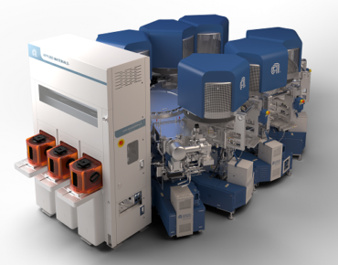
Applied Material’s Endura Clover MRAM PVD Platform
Applied Materials, the $17 billion Santa Clara-based materials engineering company for the semiconductor industry, today announced manufacturing systems enabling new memory technologies to be deposited “with atomic-level precision” within chips.
“Today’s high-volume memory technologies including DRAM, SRAM and flash were invented decades ago and have become ubiquitous in digital devices and systems,” said the company. “New memories – notably MRAM, ReRAM and PCRAM – promise unique benefits, but they are based on new materials that have been too challenging for high-volume manufacturing… The company is delivering the most advanced systems it has ever developed to enable these promising new memories to be reliably produced at an industrial scale.”
Applied Materials’ Endura platforms allow integration of multiple materials engineering technologies along with on-board metrology to create new films and structures that the company said were not previously possible. “These integrated platforms illustrate the critical role that new materials and 3D architectures can play in giving the computing industry entirely new ways to improve performance, power and cost,” said Dr. Prabu Raja, SVP/GM of Applied’s Semiconductor Products Group.
![]() Applied’s Endura Clover MRAM (magnetic random access memory, which incorporates magnetic materials found in hard disk drives and is a memory of choice for IoT devices) PVD platform is comprised of nine wafer processing chambers integrated in high-vacuum conditions, the company said, a 300-millimeter MRAM system for high-volume manufacturing for individually depositing up to five materials per chamber.
Applied’s Endura Clover MRAM (magnetic random access memory, which incorporates magnetic materials found in hard disk drives and is a memory of choice for IoT devices) PVD platform is comprised of nine wafer processing chambers integrated in high-vacuum conditions, the company said, a 300-millimeter MRAM system for high-volume manufacturing for individually depositing up to five materials per chamber.
“MRAM memories require precise deposition of at least 30 different layers of material, some of which are 500,000 times thinner than a human hair,” the company said. “Process variations of just a fraction of the diameter of an atom can greatly affect device performance and reliability. The Clover MRAM PVD platform includes on-board metrology that measures and monitors thickness of the MRAM layers with sub-angstrom sensitivity as they are created, to ensure atomic-level uniformity without risking exposure to the outside environment.”
“As an extremely fast, high-endurance nonvolatile memory, MRAM is poised to displace embedded flash and level 3 cache SRAM in both IoT and AI applications,” said Tom Sparkman, CEO of Spin Memory. “The availability of a high-volume manufacturing system from Applied Materials is a huge boost to the ecosystem, and we are thrilled to be working with Applied to deliver MRAM solutions and accelerate its adoption.”
Applied said its Endura Impulse PVD platform for PCRAM and ReRAM includes up to nine process chambers integrated under vacuum along with on-board metrology for deposition and control of the multicomponent materials used emerging memories.
“As data generation grows exponentially, cloud data centers require order-of-magnitude improvements in the speed and power consumption of the data pathways linking servers and storage systems,” the company said. “ReRAM (resistive RAM) and PCRAM (phase change RAM) are fast, nonvolatile, low-power, high-density memories that can be used as ‘storage class memory’ to fill the widening price-performance gap between server DRAM and storage.”
Applied said ReRAM and PCRAM has the potential to deliver lower cost than DRAM and faster read performance than NAND and hard disk drives. “ReRAM is also a leading candidate for future in-memory computing architectures whereby computing elements are integrated into the memory arrays to help overcome the data movement bottleneck associated with AI computing,” the company said.
“Uniform deposition of the new materials used in ReRAM memories is critical to achieving the highest possible device performance, reliability and endurance,” said George Minassian, CEO and co-founder of Crossbar, Inc. “We specify the Applied Materials Endura Impulse PVD system with onboard metrology in our ReRAM technology engagements with memory and logic customers because it enables a breakthrough in these critical metrics.”
Commenting on today’s announcement, Mukesh Khare, VP, semiconductors, AI hardware and systems, IBM Research, said, “…we see the need for these technologies increasing as the AI era demands improvements in chip performance and efficiency. New materials and device types can play an important role in enabling high-performance, low-power embedded memory for IoT, Cloud and AI products. Applied Materials’ high-volume manufacturing solutions can help accelerate the availability of these new memories across the industry.”


