


Intel Aims Xeon E7 v2 At Big Memory Workloads

Prior to earlier this year, Intel had not talked about how many cores would be in the Xeon E7 v2 chip, but had said there would be three times as much memory as the existing Westmere-EX predecessor and added that it would have features called Run Sure Technology, which it did nothing to explain. Rumors were going around late last year that Intel had actually crammed fifteen cores on the die, but this is a very unnatural number for chips and systems inasmuch as we are all used to base 2 multiples for components. Some of us, myself included, read too much into this Run Sure Technology and the rumors about fifteen cores, and assumed that the design would either be fifteen cores with only fourteen active (keeping one as a hot spare) or would show fifteen cores to the operating system but really have sixteen on the die, again with one kept in reserve as a hot spare.
As it turns out, the Xeon E7 v2 has fifteen cores, plain and simple, in three columns of five cores each. These are connected by the same overlapping double ring interconnect that was used on the Xeon E5-2600 processors, which have twelve cores in the largest configuration. In effect, the Xeon E5 and Xeon E7 are really variants of each other, rather than very different designs as was the case during the Westmere generation back in 2010 and 2011. Both the Xeon E5 and E7 chips bear the other internal code name "Ivytown" and both plug into the same LGA2011 socket, attesting to this fact. It looks like the 20 new features that are added to the Run Sure Technology basket are only turned on in the E7 variants, however.
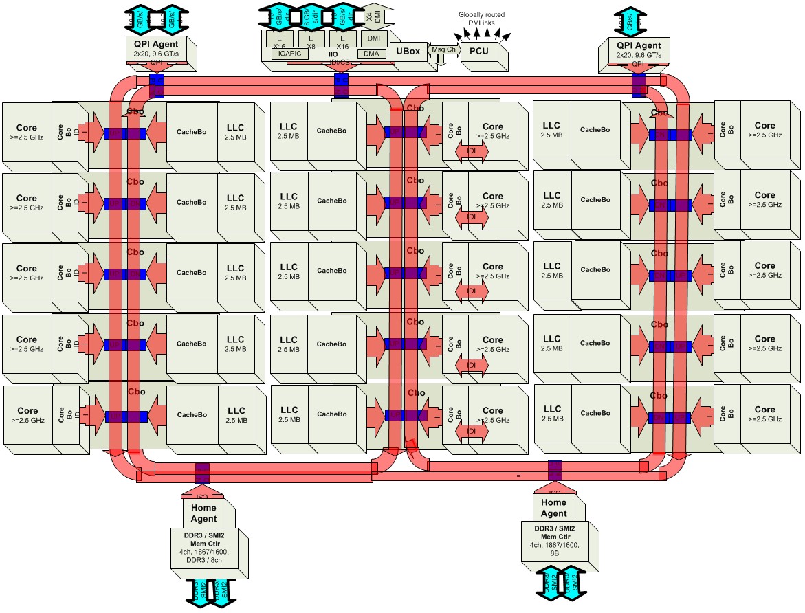
Block diagram of the Xeon E7 v2 (click to enlarge)
The Xeon E7 v2 processor has two memory controllers, and sports three QuickPath Interconnect (QPI) ports and two home agents that interface the on-chip interconnect rings to the DDR3 memory controllers and the "Jordan Creek" Scalable Memory Interface buffer chips that link the processor to the memory cards out on the system board. There are eight memory channels per Xeon E7 v2 socket, and the architecture supports three memory sticks per channel (up from two with the Xeon E7 v1 chips). The new processors support 64 GB memory sticks, while the prior generation Xeon E7 topped out at 32 GB sticks and only had sixteen sticks per socket.
The SMI Gen 2 channels implemented in the C602J chipset working in conjunction with these memory buffer chips (and collectively called the "Brickland" platform, just so you can keep the names straight) can operate in two different modes.
The first mode supports memory sticks running at 1.6 GHz and locks the memory sticks into the same speed as the SMI2 chips. This is called lock-step mode and it runs just like memory did on the combination of the Westmere-EX chip and "Boxboro" 7500 chipset. This mode is aimed at online transaction processing and other mission-critical workloads where double device data correction (DDDC) is important. (This allows the chip to map out two failed DRAM devices and correct subsequent single-bit errors.) If you are more concerned with bandwidth, such as for high frequency trading or supercomputing simulations, then there is a new performance mode that can map out only a single DRAM device and correct single-bit errors. This performance mode runs the memory interfaces at 2.67 GHz and the memory sticks at a slower 1.33 GHz. The overall effect is to give a Xeon E7 v2 more memory bandwidth.
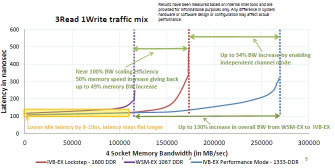
On a four-socket machine, shifting from lockstep mode to performance mode boosted the memory bandwidth by 54 percent, and this was 130 percent more than the Xeon E7 v1 chip could deliver at the same 300 nanosecond latency. This test was using a 3:1 mix of reading and writing data to main memory across the systems and using an internal Intel bandwidth testing tool.
The new Xeon E7 chips have 32 lanes of PCI-Express 3.0 I/O per socket that can be aggregated in different ways for peripheral slots, compared to a total of 72 lanes running at the slower PCI-Express 2.0 speeds with the Xeon E7 v1 chip. (That's 128 lanes for the v2 and 72 lanes for v1.)
Like their predecessors, the Xeon E7 v2 chips are available in configurations that allow for two, four, eight, or more than eight processors to be linked together in a single system image. Intel's own C602J variant of the "Patsburg" chipset glues together two, four, or eight sockets using the three QPI links that come off each Xeon E7 v2 chip. To build a larger system, server makers have to create their own node controllers and chipsets. Thus far, Hewlett-Packard and SGI are known to be working on such chipsets; there could be others.
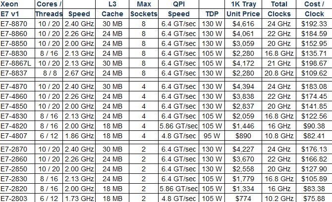
For reference, here is a table showing the Xeon E7 v1 chips:
And here are the 20 variants of the new Xeon E7 v2 processors:
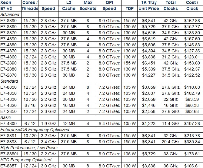
The chips are grouped in Advanced, Standard, and Basic versions, just as was the case with the Xeon E5-2600 v2 processors that launched in September 2013 for two-socket machines. Different features are activated on the versions of the Xeon E7 v2 chips. The big difference is that the QPI links run progressively more slowly as you move from Advanced to Standard to Basic, from 8 billion transfers per second (GT/sec) on the Advanced editions down to 6.4 GT/sec for the Basic chips. Incidentally, with the prior Xeon E7 v1 chips based on the Westmere cores, the QPI speeds was set at 6.4 GT/sec except for a few that ran at 5.86 GT/sec or 4.8 GT/sec.
Chips with an 8800 designation are aimed at machines with eight sockets, those with the 4800 designation go into four-socket machines, and those with the 2800 moniker go into two-socket systems. You will also no doubt notice that these new Xeon E7 v2 chips run a little hotter when pushed to their limits, coming in versions at 155, 130, or 105 watts compared to the 130, 105, and 95 watts of the Xeon E7 v1 chips.
The customer requirements outlined above requite a pretty diverse set of clock speeds, caches, and core counts, and that is why there are 20 different Xeon E7 v2 processors. In general, you pay more for more cores and higher clocks, yet still more on top of that for NUMA scalability.
For instance, it costs $6,451 for a fifteen-core E7-8890 running at 2.8 GHz aimed at eight socket boxes, but the E7-4890 with the same cores, clocks, and cache costs $222 less, and the E7-2880 costs another $168 less from that. If you look at it just based on clocks and cores, then the top-bin parts deliver 75 percent more aggregate clocks across their cores for a 50 percent price increase. But because those new Ivy Bridge cores have a lot more features and tweaks compared to those old Westmere cores – particularly for floating point math – the performance gains at the system level are much higher. (In the tables above, the total clocks figures are only given to show the relative performance and price/performance inside of a particular Xeon line. It gets more dubious across lines, particularly when cores are two generations apart as is the case in these comparisons.)
One a suite of early benchmark tests performed by Intel, here is what the actual performance gains for the top-bin parts looks like in four-socket machines:
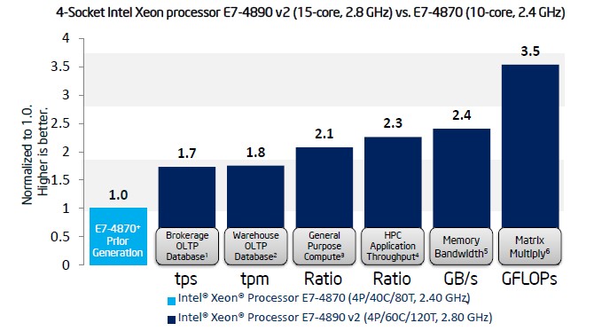
Generally speaking, customers can expect around a factor of two performance improvement per socket by moving up. A lot of that increase comes through the 50 percent increase in cores, to be sure, but all of the other tweaks add up and give the remaining performance boost. SAP HANA queries run twice as fast, and SAP's Sales and Distribution (SD) ERP test shows a factor of 1.8 performance bump. On Intel's internal server-side Java test, a four-socket box using the new Xeon E7 did twice as much work as one using the old processor; performance per watt was 2.4 times better thanks to the lower CPU idle energy consumption with the Ivy Bridge cores. The matrix math jump is so much larger because the Ivy Bridge core support AVX vector instructions (like the Sandy Bridge chips did), but the Westmere cores did not.
The more interesting comparison, perhaps, is how the Xeon E7 v2 stacks up against a two-socket Xeon E5 v2, and Intel clearly expects some customers to look at this and has run the benchmarks. Take a look:
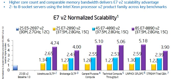
The core count and slightly higher clock speed accounts for most of the performance gains of moving from a two-socket Xeon E5 v2 system to a two-socket Xeon E7 v2, and then the NUMA scale starts from there through four and eight sockets. This comparison is all for the top-bin parts.
The more interesting variants of the Xeon E7 v2 chips are the four models at the bottom of the table above, all of which are aimed at eight-socket machines. There is a variant that has cores turned off and the clock speed radically increased with all of the L3 cache available to the 6 or 10 cores. These "frequency optimized" chips are aimed at enterprise and database workloads and are the most expensive chips in the Xeon E7 v2 lineup. Our guess is that these E7-8891 and E7-8893 chips will be aimed at SAP HANA workloads, but they could also see some action in high frequency trading or other financial modeling.
The HPC frequency optimized version, the E7-8857, is considerably less expensive and could see some action as fat nodes in supercomputer clusters. (See our report over at HPCwire for more analysis on the implications of these new processors for HPC customers.) Customers who want fifteen cores running at a low clock speed and emitting less heat and a midrange price can get the E7-8880L chip.
It sure looks like Intel wants server makers to peddle a lot of eight-socket boxes for different workloads. It will be interesting to see if they do the investment to build these machines or if the whitebox and homegrown server makers will blaze the trail.


