


MIT Prototypes Zippy Flash-FPGA Hybrid Storage Array

Researchers at the Massachusetts Institute of Technology, working with funding from server maker Quanta and flash chip maker Samsung, are combining flash storage and field programmable gate arrays in a new way that is yielding a peppy and scalable storage cluster that rivals that bandwidth and low latency of very high-end storage area network or clustered file systems.
The project, called BlueDBM, is based on relatively old FPGAs from Xilinx and flash cards from Micron Technology, but the resulting four-node prototype is delivering decent performance stats. Therefore the MIT researchers – Sang-Woo and Jun, Ming Liu working with Kermin Elliott Fleming of Intel – are working on a second prototype with sixteen nodes and more modern FPGAs and flash memory cards that will show significantly higher bandwidth and lower latency across that cluster as it feeds applications.
The researchers will be presenting their findings in a paper at the 22nd annual ACM/SIGDA International Symposium on Field-Programmable Gate Arrays, which takes place later this month in Monterrey, California.
Non-volatile NAND flash memory can be accessed in tens of microseconds, and that is around three orders of magnitude better than the seek time of a disk drive. And while flash is slower than main memory, like disks it retains its data even when it loses power. This is something that main memory cannot do. It is not as simple as just putting flash memory sticks in a system where a disk drive used to be. Flash has such higher I/O rates that it can quickly flood controllers that are used to handling perhaps a dozen or so relatively slow disk drives. Flash is so fast, in fact, that now the storage network (either between devices that create a storage cluster or between the storage and the server where applications are running) is a major bottleneck where, with disk drives, it had ample capacity in the past. The software stack relating to linking the operating system and applications to storage is also a bottleneck.
The BlueDBM, short for Blue Database Machine, was designed to work around these limitations. The prototype is fairly simple, in fact:
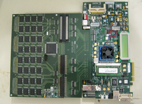
This is the pairing of a Xilinx ML605 board, which has a Virtex-6 FPGA chip on it. This FPGA is programmed to act as a flash controller as well as a compute accelerator for certain functions. The one that MIT tested was a word count accelerator, which was able to count the number of times a word appeared in a dataset that was streaming through the controller. The 16 GB of flash storage on the prototype is implemented in four parallel buses, each with eight 512 MB Micron SLC flash chips. These flash chips top out at around 25 MB/sec of throughput, which the researchers say their controller can easily handle.
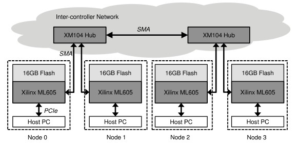
The neat bit is that the MIT techies are taking the 5 Gb/sec SERDES interconnect on the FPGAs and using it to link the FPGAs together into a distributed controller. Each FPGA only has two such interconnect ports, so some latency is necessarily introduced by the use of a pair of Xilinx XM104 hub connectors to link the FPGAs to each other. The four PCs that acted as hosts in the prototype, which use up half the SERDES links, were running Canonical's Ubuntu Linux and used the FUSE file system. Here's the block diagram of the prototype:
Even with this relatively old equipment, the BlueDBM clustered flash array was able to drive 450 MB/sec of bandwidth, or about 70 percent of the peak bandwidth of the FPGA network, with an average packet latency of 5 microseconds. The average latency out to client applications from the device is 70 microseconds. This, says the MIT team, is an order of magnitude better than the CORFU flash array prototype put together by Microsoft Research recently.
Based on early tests, the researchers think that they can scale the BlueDBM flash cluster to hundreds of nodes with an "average-case performance" that rivals that of commodity SSDs plugged into a server and a "best-case performance" that rivals that of a PCI-Express-based flash memory card. The latency across the FPGA SERDES network is very low, and the prototype scales nearly linearly. With more modern FPGAs and flash memory chips, MIT thinks it can do a lot better. Xilinx has donated twenty VC707 FPGA boards to the cause, and the plan is for each hybrid FPGA-flash node to deliver more than 1 GB/sec of storage bandwidth; the links to the servers off the array will deliver more than 3 GB/sec, if all goes well. Depending on the flash chips that MIT can get its hands on, the second-generation BlueDBM should have between 16 TB and 32 TB of capacity and be useful for testing on relatively large datasets.


